1. KIOXIA SLC Flash Series
KIOXIA's SLC NAND can write a large amount of data at high speed. It is a 1-bit/cell non-volatile memory with high endurance of erase and write cycles and reliability. The KIOXIA SLC NAND flash product series offers a variety of capacity and package options to meet different needs in the embedded market.
KIOXIA's SLC NAND flash is divided into two major series: RAW and BENAND™. Both are single-level cell SLC Nand flash based on the 24nm process, and the chip pins and interfaces are compatible. The BENAND series flash has a built-in ECC (Error Correcting Code) with an 8-bit/528-byte error correction capability (512B main field + 16B spare field), eliminating the ECC burden on the main control chip side.
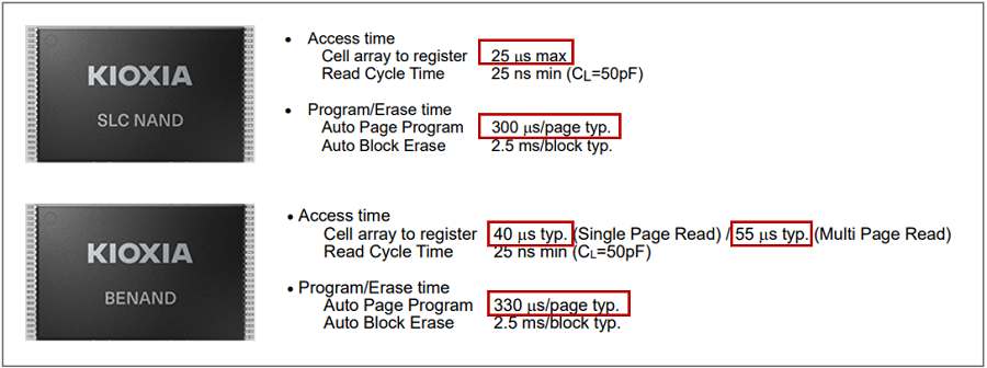
Figure 1: Flash Chip with Integrated ECC Function, with a Slight Decrease in Speed
As shown in the above figure, KIOXIA's BENAND series chips are compatible with the hardware interface of the SLC NAND series. Due to the addition of the ECC error correction hardware circuit, the data read performance index of the storage chip has decreased slightly, and the manufacturing cost of the chip has increased.
KIOXIA SLC NAND flash chips have high endurance of erase and write cycles and reliability. The capacity range covers from 1Gb to 16Gb, including various operating voltages, operating temperatures, and packages. The specific model specifications are shown in the following table:
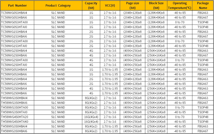
Figure 2: KIOXIA SLC NAND Flash Chip Series
KIOXIA's BENAND™ series is SLC NAND flash with a built-in ECC. The BENAND™ series is compatible with the interface of the RAW SLC NAND series flash. It has a built-in ECC hardware function, eliminating the ECC burden of the main control, and the capacity ranges from 1Gb to 8Gb. The specific model specifications are shown in the following table:
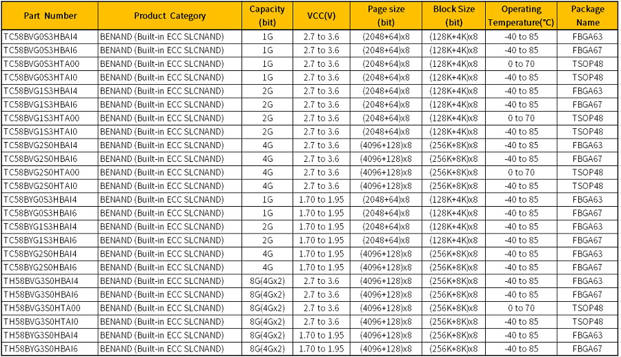
Figure 3: KIOXIA BENAND Flash Chip Series
In the market where price sensitivity and large-capacity storage requirements exist, more economical TLC and QLC types of Nand flash are likely to be adopted. However, SLC NAND flash is still an integral part of the entire flash market. Its high durability makes it very suitable for various application scenarios in consumer, industrial, network communication, automotive, etc., which have very high requirements for reliability and lifespan.
2. Development of Flash Memory Technology
In 1967, Dawon Kahng and Simon S. M. Sze of Bell Labs invented the "floating-gate transistor". In 1971, Intel engineer Dov Frohman invented the ultraviolet erasable EPROM based on the floating-gate transistor. In 1977, an engineer from Hughes Corporation in the United States invented the electrically erasable EEPROM. In 1980, Fujio Masuoka of Toshiba Corporation invented the NOR (NOT-OR) memory chip with adjacent floating-gate transistors connected in parallel, and in 1987, he iterated to the floating-gate transistor series NAND (NOT-AND) flash with a simplified circuit. The storage density of the same wafer area can be increased by 2.5 times, and the cost is greatly reduced.
The new Nand Flash structure brought by Toshiba Corporation emphasizes reducing the cost per bit while bringing higher performance. Therefore, Nand Flash does not use the random read technology of memory but reads data in the form of reading one block at a time, usually 512 bytes at a time. At the same time, it uses a non-linear macro cell mode internally, providing an inexpensive and effective solution for the realization of large-capacity solid-state memory.
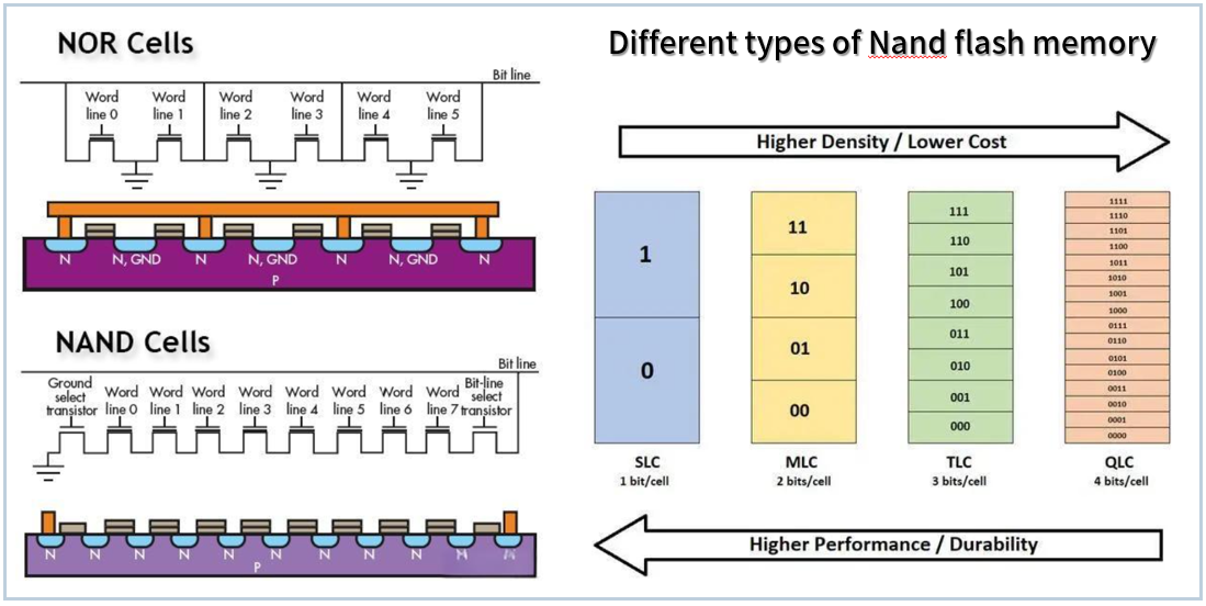
Figure 4: Differences between Different Types of NAND Flash
According to the density difference, the currently common flash memory particles of NAND flash are mainly divided into four types: SLC, MLC, TLC, and QLC. Among them, SLC is also known as single-level storage, that is, each cell can store 1bit of information (1bit/cell). The erase and write lifespan of SLC is the longest among the five types of particles, which can reach about 100,000 times. It has the fastest read and write speed, the most accurate read and write data, the best quality, and is also the most expensive particle. It is applied in consumer electronics, the Internet of Things, automotive, industrial, communication, and other related industries with high reliability requirements.
3. Flash Memory ECC Error Correction Technology
Due to the differences in circuit structure, the probability of bit flipping (a single bit flipping) occurring during the operation of NAND flash is much higher than that of NOR flash. The possible factors are as follows:
(1) Instability of storage cells caused by manufacturing defects;
(2) With the increase in the number of read and write operations, the storage cells degrade, and the probability of errors increases;
(3) Environmental factors such as temperature, humidity, and electromagnetic interference may lead to data errors;
The data integrity and reliability of storage chips are of vital importance. When errors occur in important file data, it will bring catastrophic impacts to the system. The ECC (Error Correcting Code) technology can effectively solve this problem. Therefore, when using NAND Flash, it is usually necessary to add an ECC error correction algorithm. Commonly used coding technologies include Hamming code, BCH, and LDPC:
(1) Hamming code: It has low performance and can be implemented with only a very small amount of hardware circuit (5-level XOR gate).
(2) BCH: An early error correction code with an error correction capability of 80bit/1024 bytes, used in data storage and communication protocols.
(3) LDPC: It approaches the Shannon limit performance in a low signal-to-noise ratio environment. The ECC error correction capability is more than three times that of the BCH code, and it has become the mainstream error correction code at the bit level, with wide applications.
SLC flash has high reliability, so the requirements for the ECC error correction capability of the processor/controller are very low. Usually, only 4/8bit error correction is required to meet the needs of high durability applications, and a simple Hamming code can meet the requirements. MLC flash usually requires an ECC capability of more than 40bit, and BCH coding is usually used. TLC flash requires an ECC capability of more than 120bit, and LDPC coding must be used to achieve better results.
In devices such as industrial control and smart wearables, they have low requirements for storage capacity but high requirements for real-time performance, reliability, and stability. And usually, the processors of these devices do not have sufficient computing power like those of PCs to implement complex ECC error correction algorithms. In this case, it is recommended to select SLC flash with an ECC function, so that the ECC error correction is completed by the flash hardware itself, and the host side only needs to perform simple functions such as bad block management, wear leveling, and garbage collection.
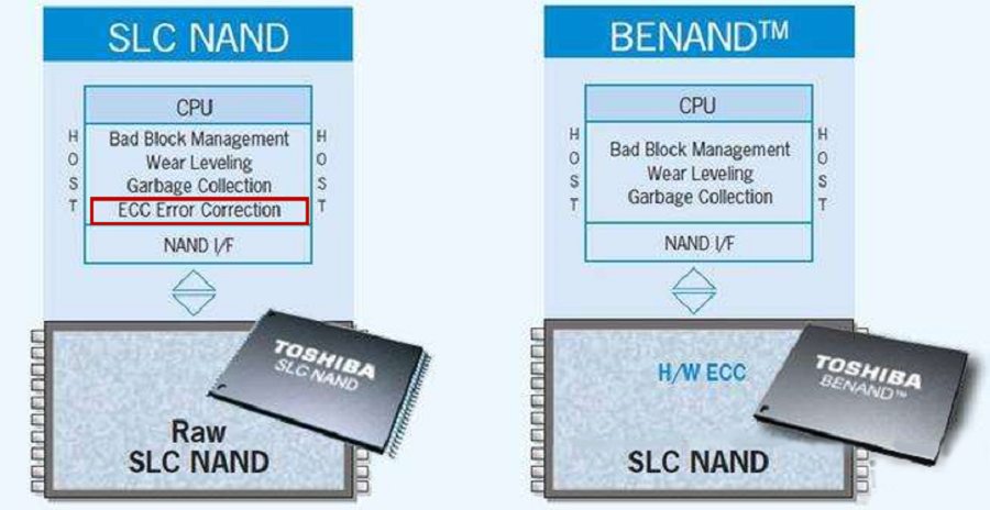
Figure 5: Flash Chips with Integrated ECC Function are More Friendly to the Controller
Integrating ECC into NAND flash enables the memory chip to manage ECC directly by itself, effectively simplifying the system design. However, the cost is an increase in the hardware cost of the storage chip and a decrease in the read performance. However, since the data read and write speed of SLC Nand flash itself is very fast, the application of ECC technology in SLC particles mainly ensures the accuracy of data storage, reading, and writing, and has a negligible impact on performance.
4. Conclusion:
According to the statistical data of the research institution QYResearch, the global SLC NAND flash market size is expected to be 2.36 billion US dollars in 2022. High-reliability and high-performance storage requirements in industries such as industrial, medical, automotive, communication, and military have promoted the market of SLC NAND Flash. In the future, with the popularization of the Internet of Things and edge computing, the demand for high-performance, low-power, low-latency, and high-reliability storage solutions will increase.
KIOXIA, formerly known as the Toshiba Memory Group, was separated from Toshiba Corporation in 2017 and has become a global leader in memory solutions, committed to the development, production, and sales of flash memory and solid-state drives (SSDs). KIOXIA's innovative 3D flash memory technology BiCS FLASH™ is shaping the future storage methods for many high-density applications, including high-end smartphones, PCs, SSDs, automotive, and data centers, etc. KIOXIA's SLC high-performance flash product series is also a representative of quality and performance in the industry and is widely used in various high-performance electronic devices.
For more information about KIOXIA storage chip products, please contact us.


