The NAND structure can provide extremely high cell density, achieving high storage density, and also has fast writing and erasing speeds. The cell size of NAND Flash is almost half that of NOR devices. Due to the simpler production process, the NAND structure can offer higher storage capacity within a given space, thus correspondingly reducing the price per unit of storage capacity. Nand-flash memory has advantages such as large capacity and fast rewriting speed, making it suitable for storing a large amount of data, and it has been increasingly widely used in the industry.
1. Introduction to KIOXIA Company
KIOXIA is a global leader in memory solutions, dedicated to the development, production, and sales of flash memory and solid-state drives (SSDs). Toshiba Corporation invented NAND flash memory in 1987. In April 2017, the predecessor of KIOXIA, the Toshiba Memory Group, was separated from Toshiba Corporation, creating advanced storage solutions and services that can enrich people's lives and broaden the horizons of society. KIOXIA's innovative 3D flash memory technology, BiCS FLASH™, is shaping the future storage methods for many high-density applications, including high-end smartphones, PCs, SSDs, automotive, and data centers, etc. Its retail products cover various flash memory products such as memory cards, USB flash drives, and solid-state drives, aiming to enable end-users to store their digital lives anytime and anywhere.
Figure 1: KIOXIA Memory ICs
2. KIOXIA BiCS Flash 3D Flash Memory Technology
Kioxia's BiCS FLASH™ is a three-dimensional (3D) vertical flash memory cell structure. This structure enables it to exceed the capacity of 2D (planar) flash memory. Kioxia's TLC 3-bit/cell 1Tb (128GB) BiCS FLASH is the first of its kind in the industry, improving both the writing speed and the reliability of the number of erase and write cycles. The company also offers 1.33Tb BiCS FLASH™ that uses 4-bit/cell, four-layer cell (QLC) technology. This is the first 3D flash memory device to adopt this technology.
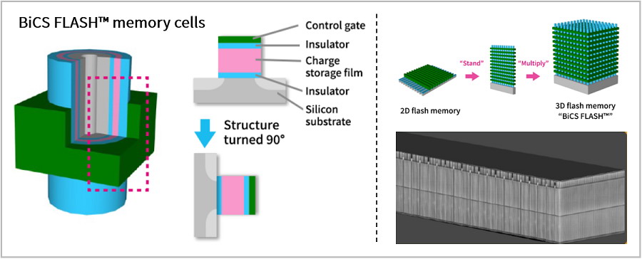
Figure 2: KIOXIA BiCS Flash Memory Cell
KIOXIA's BiCS FLASH™ provides 1 terabit (Tb) 3-bit/cell, three-layer cell (TLC) and higher-capacity QLC technology, achieving a larger chip capacity. Kioxia has achieved the industry's largest single-chip capacity of up to 1.33 terabits (Tb), and its 16-chip stacking architecture can achieve a maximum single-package capacity of up to 2.66 terabits (Tb).
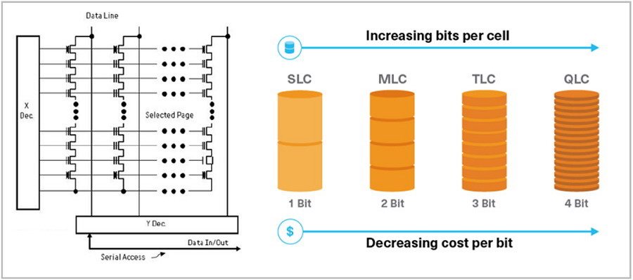
Figure 3: Circuit Structure and Technological Evolution of Nand Flash Memory
3. Selection of KIOXIA NandFlash Memory ICs
In 1987, KIOXIA invented the world's first NAND flash memory. Then, in 2007, we took the lead in developing 3D flash memory technology, enabling us to increase the capacity of flash memory. Today, this technology plays an important role in changing the lives of people around the world. KIOXIA provides a variety of flash memory products to meet various needs.
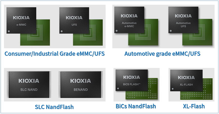
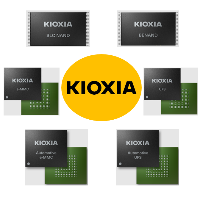
Figure 4: KIOXIA's Flash Memory Product Series
3.1 KIOXIA SLC Flash Memory
The SLC (Single Level Cell) chip is the most basic type in flash memory technology, with each storage cell storing only one charge. This design allows SLC chips to achieve high-speed reading and writing and multiple erasing and writing operations, with the number of writing times reaching more than 100,000 times. Therefore, SLC NAND flash memory remains an integral part of the entire flash memory market. Its high durability makes it very suitable for various consumer and industrial applications that have very high requirements for reliability and lifespan.
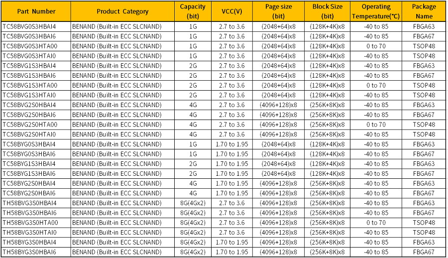
Figure 5: KIOXIA SLC Flash Memory ICs
3.2 KIOXIA e-MMC
KIOXIA's high-performance e-MMC product series is equipped with an integrated controller that supports a high-speed memory interface compliant with JEDEC version 5.0/5.1, eliminating the need for the host processor to directly control the flash memory. For many applications that cannot migrate to the latest generation of UFS due to lower density requirements or the host processor not yet supporting the UFS interface, e-MMC remains an important solution. Kioxia e-MMC is manufactured using 15nm process technology or the more advanced BiCS FLASH™ 3D flash memory, making it highly suitable for a wide range of applications that require e-MMC as an embedded memory solution.
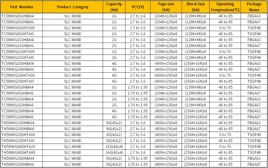
Figure 6: KIOXIA Consumer/Industrial e-MMC Product Series
3.3 KIOXIA UFS
UFS uses a serial interface, reducing the number of signal pins and simplifying the wiring. It supports full-duplex operation, enabling simultaneous reading and writing between the host processor and the UFS device, bringing ultra-high-speed read/write performance, low power consumption, and fast application startup times, greatly improving the overall system performance and enhancing the performance of mobile devices. KIOXIA's UFS solutions comply with JEDEC/UFS versions 2.1/3.0/3.1 and integrate the company's BiCS FLASH™ 3D flash memory with the controller in a JEDEC standard package, meeting the needs of various digital consumer products.
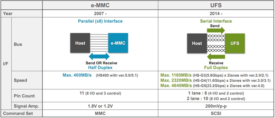
Figure 7: Comparison of e-MMC and UFS Interfaces
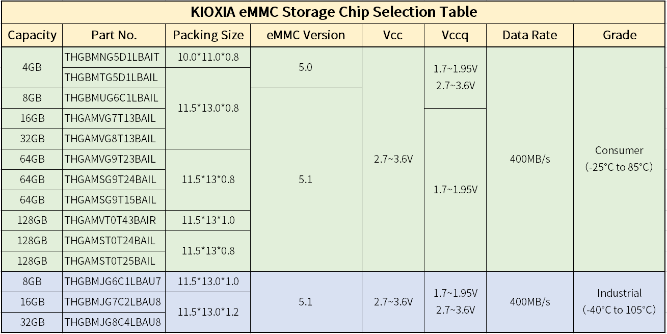
Figure 8: KIOXIA eMMC Storage Chip Selection Table
UFS 4.0 incorporates MIPI M-PHY 5.0 High Speed Gear 5 and UniPro2.0, supporting a theoretical interface speed of up to 23.2Gbps per channel or up to 46.4Gbps per device. UFS 4.0 is backward compatible with UFS 3.1, so existing platforms can use the latest generation of flash memory technology used in UFS 4.0 while combining all existing UFS 3.1 functions. The sequential read and write performance of UFS 4.0 devices has increased by approximately 100% and 95%, respectively.
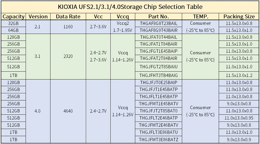
Figure 9: KIOXIA Consumer & Industrial UFS2.1/3.1/4.1 Storage Chips
3.4 Designed for Speed: Low Latency and High Performance Storage Class Memory (SCM) Solution
Due to the growing market demand for flexible and affordable storage class memory (SCM) solutions, KIOXIA has developed a flash memory, XL-FLASH, with extremely low latency and high-performance characteristics. XL-FLASH is designed to fill the performance gap between volatile memory (such as DRAM) and current flash memory. Like all flash memory, XL-FLASH can retain data when the power is disconnected. The second-generation XL-FLASH with MLC functionality is in mass production.
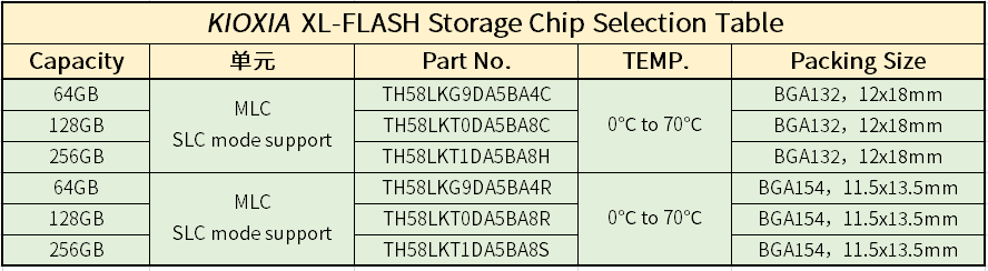
Figure 10: KIOXIA XL-FLASH Storage Chip
3.5 Automotive-grade UFS and e-MMC Chips
KIOXIA offers a variety of automotive application UFS(1) product lines with different capacities, capable of meeting the increasingly complex data storage needs of automotive applications. KIOXIA's automotive UFS can operate within a temperature range of -40 to +105°C, meets the requirements of AEC-Q100 Grade 2(2), and provides high reliability to meet the needs of demanding automotive applications.
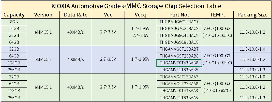
Figure 11: KIOXIA Automotive-grade e-MMC Storage Chip
In 2024, KIOXIA launched the industry's first automotive UFS 4.0 to support the development of the next-generation in-vehicle infotainment systems and ADAS (Advanced Driver Assistance Systems). The automotive UFS 4.0 has an interface speed of up to 46.4Gbps, meeting the needs of automotive applications for faster loading times, including deep 3D mapping, richer in-vehicle information and entertainment systems, and ADAS.
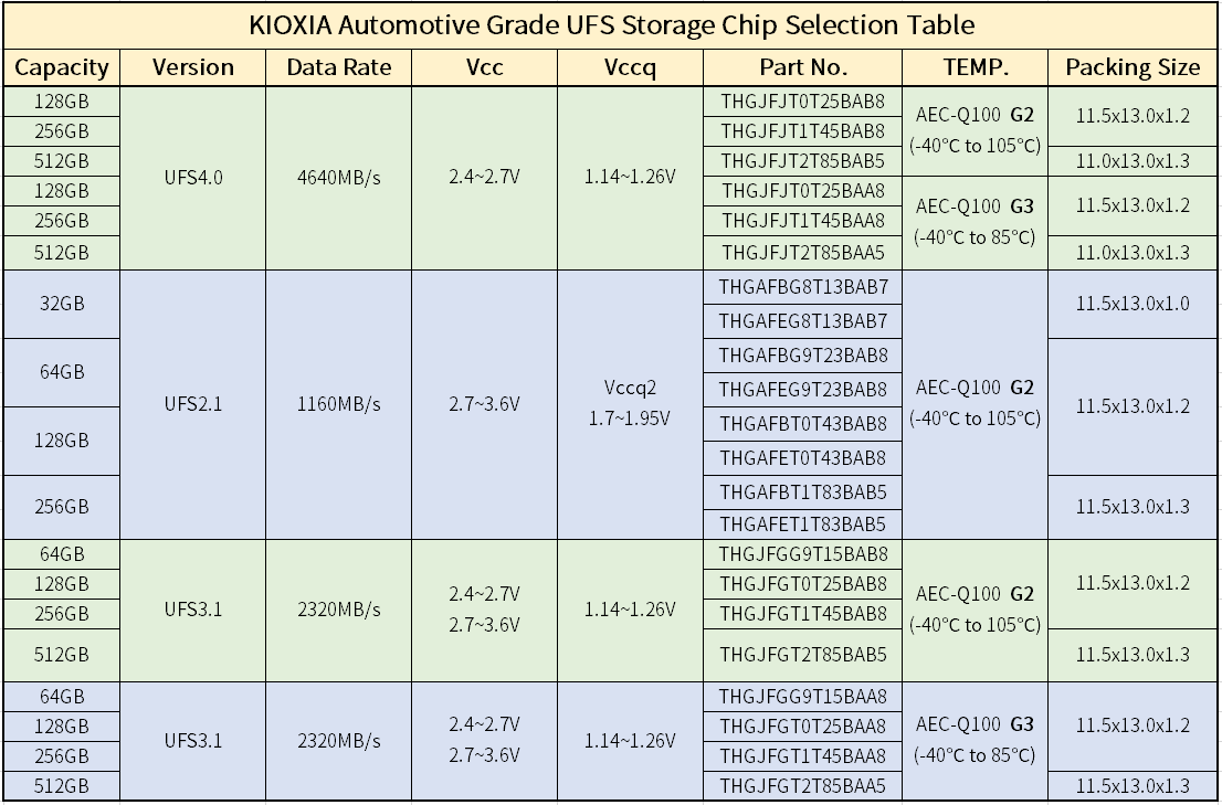
Figure 12: KIOXIA Automotive-grade UFS Storage Chip
4: Application Scenarios
From automotive applications, to high-performance personal computers, to large-scale data centers, and cloud services, KIOXIA's storage solutions with high performance, high reliability, and low latency can all provide support and help businesses realize their expected potential.
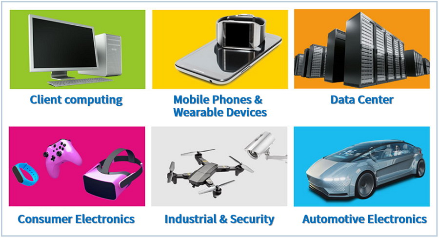
Figure 13: Main Application Scenarios of KIOXIA Storage Chips
For more information about KIOXIA storage chip products, please contact us.


